Senseeker Establishes In-House Wafer Testing Capability
July 2, 2020 | Santa Barbara, CA
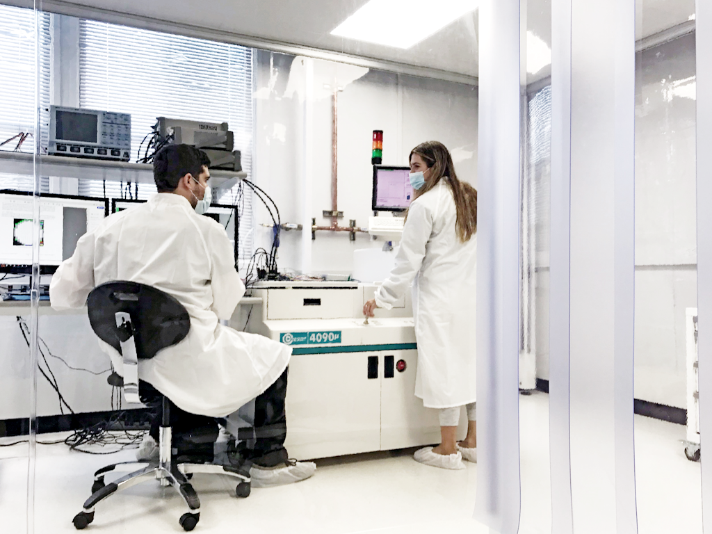
Senseeker, a leading innovator of digital infrared image sensing technology, can now respond to customer requirements more quickly by providing a cleanroom-based wafer probe capability that supports quick-turn, in-house wafer testing.
The standalone Senseeker facility in Santa Barbara is equipped to perform testing from semiconductor die to assembled ICs under an extreme range of conditions, including cryogenic and high-temperature oven testing. In addition to reducing wafer delivery cycle times, Senseeker is equipped to support specialized customer test, failure analysis and manufacturing yield enhancements.
“The in-house wafer screening is an important step in the evolution of the company. Senseeker has recently started selling commercial products and this capability allows us to quickly process customer orders,” said Kenton Veeder, President at Senseeker. “We can bring up new designs efficiently and verify our novel architectures with the whole design team onsite, bringing satisfaction to our team and value for our customers.”
The new Electroglas 4090u wafer prober provides fully-automated state-of-the-art die probing capability. The dedicated Senseeker test team has tested die, partial wafers and full wafers in the recently installed class 10,000 clean room environment.
About Senseeker
Senseeker is a wholly US owned transducer IC semiconductor company that specializes in the design of stateof-the-art digital imaging sensors and readout integrated circuits for hybrid infrared image sensing arrays. Senseeker's products and IP enable designers to produce world class infrared image sensing solutions. Read more at https://www.senseeker.com.
Media contact: info@senseeker.com | 1 (805) 617-0337
Press Release # PR-20200702